The time is UP!

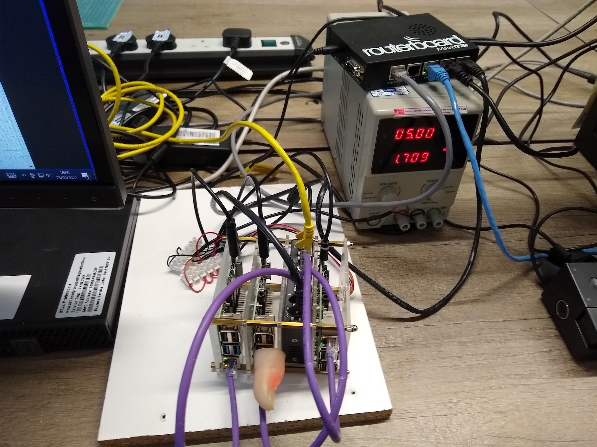
Followers of this blog will know that I have an interest in the whole ecosystem of Raspberry Pi “compatible” boards. By now I have quite a selection.

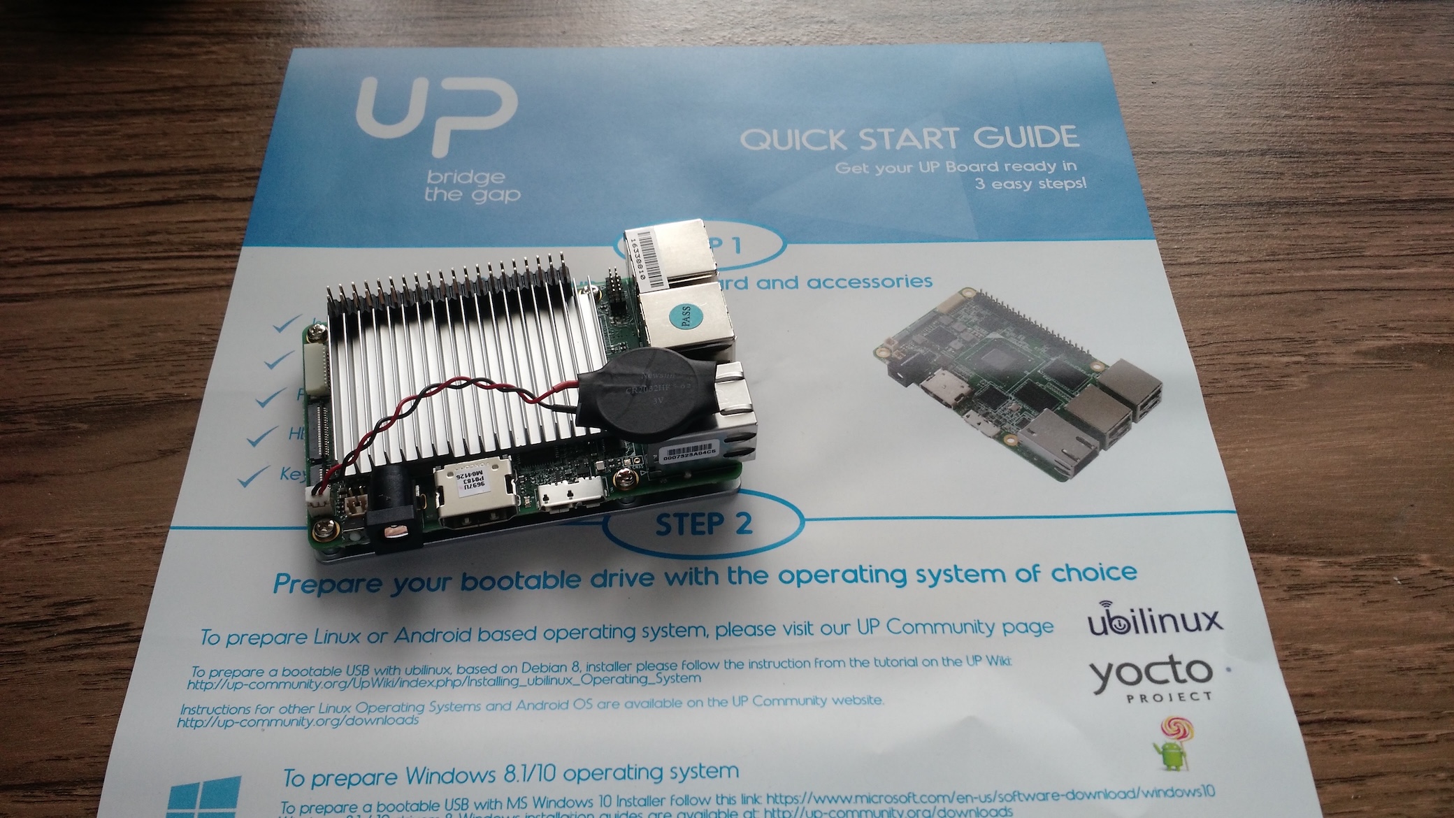
Mostly, the boards I have in my collection are ARM-based, often using a System-on-Chip (SOC) from AllWinner rather than the Broadcom devices used by the official Raspberry Pi boards, but occasionally something a bit different is produced. Last October, I backed the Up board on Kickstarter. There is always a risk (and usually a delay) with crowd-sourcing, so I was hardly surprised when the expected delivery date slipped from Jan/Feb 2016. Today, however, my UP board arrived!

UP board and instruction sheet

This board is particularly interesting, as it has a reasonably-modern Intel processor, but in something pretty close to the Raspberry Pi form factor. I have yet to try it out, but with a 1.8 GHz quad-core, 64-bit CPU and 2GB RAM it should easily handle generic PC linux distributions. What support for the GPIOs and other hardware on the Raspberry Pi header will be like is less obvious.

The publicity photos for the board all look very Raspberry-Pi-like, but the manufacturer seems to have had some problems with heat dissipation – the board I received is almost hidden behind two huge heatsinks. A finned one on top covering most of the circuit board, and a full-sized plate on the bottom, which co-incidentally uses up all four of the “HAT” mounting holes. Just to add to the clumsy look, there is also a clock battery perched on the ethernet socket with a sticky pad.

I don’t immediately have a project which might need an embedded x86 PC, though, so for now, this one will go into the collection…

BURP part 1

I have been enjoying reading a blog by Ken at Sustainable Suburbia recently, and one post in particular sparked me into action. Not because of its main topic (although that is thought-provoking, too) but because of the mention of an odd early programming language named “BURP” (Basic Using Reverse Polish).

Sufficiently intrigued by this idea, I read around a bit, and decided that I would have a go at producing a version of this. There’s not a wide range of information about the BURP language or system, but there are a few articles from “Wireless World” magazine in the late 1970s and early 1980s which describe the design of both the BURP language and the “Psi-Comp 80” home computer which used it. The key to the system seems to be the National Semiconductor MM57109 “Number-Oriented Processor” which did most of the mathematical work, alongside a more familiar Zilog Z80, so I have started by getting to grips with this quirky co-processor.

Fell free to follow along with the development on GitHub.

Day Zero

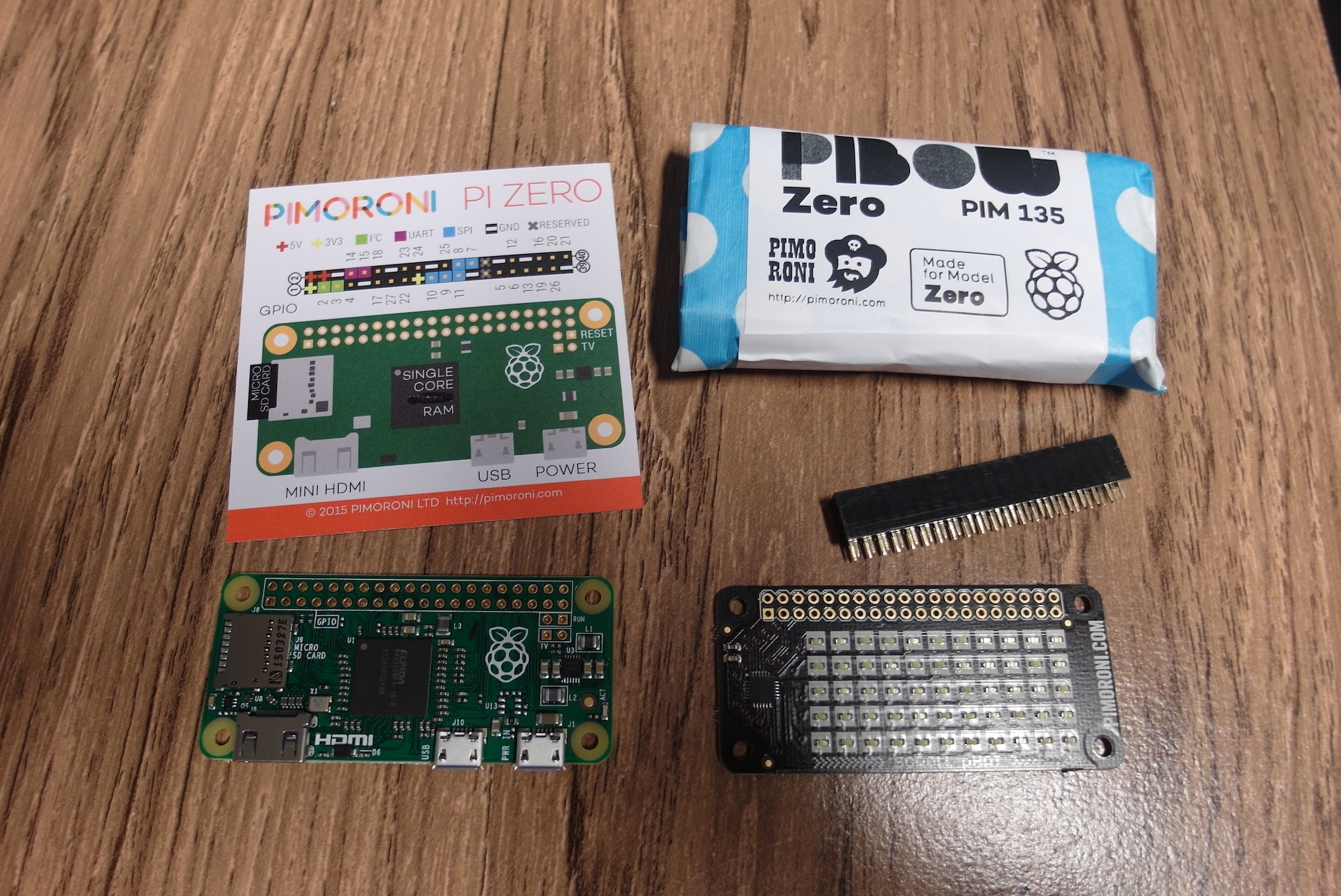
As you might imagine, if you have read many of these posts, I was very excited to hear of the launch of the Raspberry Pi Zero, and ordered one straight away. It arrived this morning, so I am now the proud owner of a Zero, and also a case and the first ‘pHat’ from the lovely people at Pimoroni

Raspberry Pi Zero and accessories

Freescale Kinetis KwikStik (part 2)

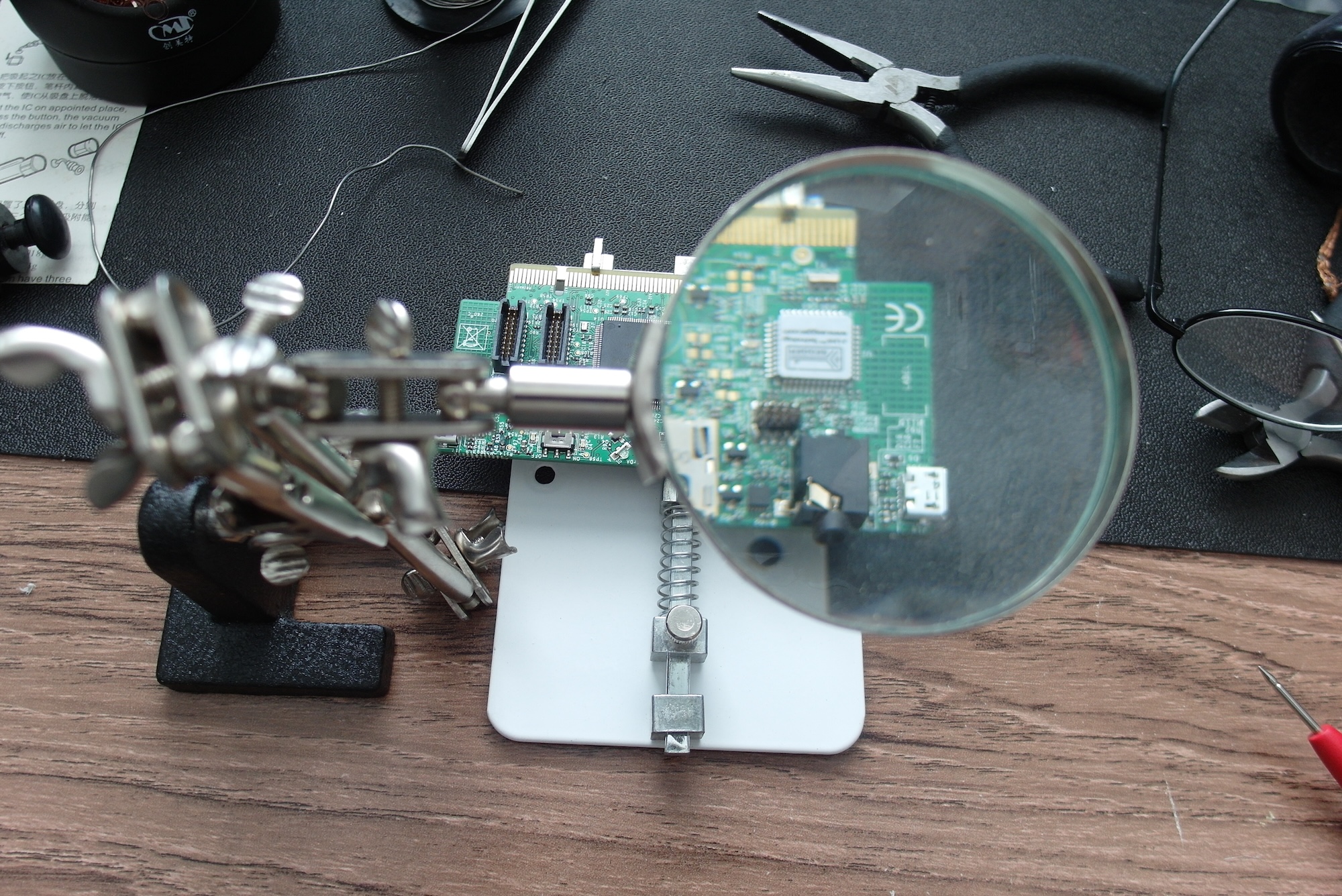
My previous post ended with me waiting for delivery of a surface-mount SWD connector so I could turn a Freescale Kinetis KwikStik K40 into a Segger J-Link compatible debug probe. I placed an order with Farnell UK for an appropriate connector, and it arrived the next day.

SAM_0601

Soldering the connector was surprisingly difficult. I had assumed that it would be about as hard as the NXP LPC812 and Freescale KE04 chips which I had recently soldered onto adapter boards, but it turned out to be much more tricky. I think there were several contributing factors. The most obvious factor was the location of the connector, tucked in between an audio connector and the Segger chip. Although some of the pins had clear access for a soldering iron, that was certainly not true for all of them. There was also the matter of my soldering iron and its tip. I have been using the same Antex iron on and off since the 1980s, most of that time with the same tip. It has served me very well for through-hole soldering, wire tinning and so on, but I have now come to the conclusion that the tip is just too large for delicate work such as this.

Finally, of course, there is my own skill level and experience. This task was plagued by solder bridges between pins and required lots of continuity beeping and solder-wicking to get things clean.

  • Top tip: two of the pins on the 10-pin SWD connector, which happen to be adjacent, are both connected to ground. However much solder you wick, you’ll never get them isolated. Sigh.

After reading up, it seems that I might have had better luck had I spread on some extra flux, rather than just relying on the flux core in the solder.

SAM_0603

Eventually I did get to the point where the continuity testing agreed with what I was expecting, so I gave the board a try. I connected the USB lead to my computer, and the small SWD connector through an adapter to my custom KE04 board. I started by trying to program the chip from the Freescale KDE software, much as I had using the FRDM board as a debugger. This did not work, giving some fairly cryptic error messages. I double-checked the connections, tried lots of combinations of restarting and changing the position of the target switch on the KwikStick, but sill only uninformative errors. Luckily, the Segger drivers come with some tools which connect directly to the debug probe and give much more information.

In particular, two useful programs are J-Link Commander and J-Link Configurator. J-Link Commander is a command-line tool which looks for a Segger J-Link debug probe attached either by USB or ethernet. If it finds one it displays some information and waits for textual commands to control it. J-Link Configurator tries a bit harder, and will find multiple probes if more than one are attached. Any J-Link devices it finds are listed, along with driver and firmware version numbers and, where possible, the option to update software. The combination of these two tools eventually enabled me to get the KwikStik working as a debug probe. I tried a lot of things, but I’m pretty sure the following things did need doing:

  • Remove all other J-Link compatible devices before starting. Although these tools should work with multiple debug probes, I had a lot more problems with more than one attached.
  • Attach the probe and wait for any driver installation to complete before starting either of the J-Link tools. (I seemed to have better luck when I attached the device to a different USB port which had not been used by another J-Link.)
  • Check that the target switch on the KwikStick is in the correct position, and pay attention to the output from J-Link Commander. If the switch is in the wrong position, the description of the target device will list a Cortex M4, rather than the actual target device (in my case a Cortex M0+ which reports as Cortex M0). If it shows the wrong target, power off the target and the KwikStik, unplug the USB, switch the switch, re-plug and re-start.


    K40 Segger

    K40 Segger ext

  • Depending on what versions you have, you are likely to need to update the KwikStik firmware. This is a simple process using J-Link Configurator, and only took a few minutes. Once done, power off and unplug everything, then start again.

With any luck, this set of steps, in some order, should help you get a working KwikStik Segger J-Link Lite debug probe, licensed for use with all Freescale ARM chips.

As a twist to the story, I was determined to get this working, but I did have a fall-back position. In the same delivery from Farnell, I also got a Segger J-Link EDU. As pointed out by Erich in the comments to my previous post, this is reasonably priced, and licensed for use in educational and non-profit situations. That works for me. In the unlikely event that I ever end up making any money from this blog, I’ll be more than happy to rush out and buy the full commercial license. In the meanwhile, I now have three kinds of Segger, each with different capabilities and licence terms.

SAM_0602

three-jlinks


Freescale Kinetis KwikStik (part 1)

Although I had some success with using the Segger firmware on a Freescale FRDM board to program a KE04 microcontroller on a header board recently, I was very aware that I was being naughty. The terms of use for the Segger firmware make it clear that it is only for programming and debugging genuine Freescale FRDM development boards, and should not be used for custom hardware. I don’t like to break such terms, and the Segger folks deserve to be rewarded for the effort they put into making such useful tools. So I have ordered a real Segger™ J-Link™ and hope to have a lot of fun with it. In the meanwhile, though…

Kinetis KwikStik box

My collection of microcontroller development boards is sufficiently rambling, that the addition of a new one is hardly news. However, I recently noticed that Freescale also sell an interesting development board for their K40 series of Cortex M4 chips. It comes with a variety of peripherals on the board including a graphic LCD, capacitive button pads, microphone, audio output jack and even a rechargeable battery. Most interesting, though, is that it includes Segger debug firmware with much less restrictive usage terms.

The Freescale page for the board states:

The on-board Segger™ J-Link™ debug interface allows the user to evaluate the features of the on-board K40 MCU or to develop, debug and program their own target hardware based on any Kinetis MCU.

This seems just what I want for now. And at around £30-35 from the usual suppliers it’s about 10% the price of the Segger J-Link Base model!

SAM_0594

On opening the box, the board itself comes in a cute orange silicon sleeve with branding from Freescale and “Pounce Consulting” who seem to be a design company in Mexico. Plugging in a micro-USB power connector starts up some demo software including a kind of low-res monochrome tetris game and a sound recorder. I found this software very confusing and frustrating to use with the un-labelled capacitive button pads, and all I could get was noise from the sound recorder, so I think it’s probably best used for development or as a debug probe rather than as an application platform on its own.

SAM_0596

SAM_0595


The silicone skin is a bit tricky to peel off, but once it is removed you can see that you get quite a lot of stuff for your money, The main MCU is the 144-pin K40X256VLQ100 with a Cortex-M4 core running at 100MHz, 256K of Flash, 256K of RAM and loads of i/o including USB and 6 UARTs. I/O pins are brought out to an edge connector and some sockets specific to the Freescale TWR development framework and there’s an array of interfaces along the top. Two micro USB, micro SD socket and infra-red. On the other side there’s the large (if low-resolution) display panel, a tiny electret microphone capsule and a little buzzer.

SAM_0597

The annoying part of this, however, is that you can’t use it as a debug probe out of the box. There’s a lovely Segger-branded debug chip, there’s a handy switch to flip it from internal to external target (no track-cutting, hurrah!), but the vital connector for the external JTAG/SWD lead is not populated. Worse than that, it’s not even the same connector as on the other boards – those are all through-hole connectors and this one is surface mount, so I need to order a connector specially. It also looks like I will need to ‘adapt’ the silicone skin if I plan to use it, as there is no obvious hole for the debug cable.

I won’t be able to test this out as a debugger until I get and fit the new connector. Sigh.

So I give this board a smile for features and price, so-so for the demo software and a scowl for the lack of a populated debug connector.

ARM Cortex-M board from scratch part 3: Kinetis KE04

If you have read my previous post in this series, you’ll know that I had mixed feelings about the LPC810 and LPC812 chips from NXP. They are certainly simple and flexible in use, but without a stable and predictable technique to program them I just ended up more frustrated. However, I impressed myself by successfully soldering the surface-mount TSSOP package of the LPC812.

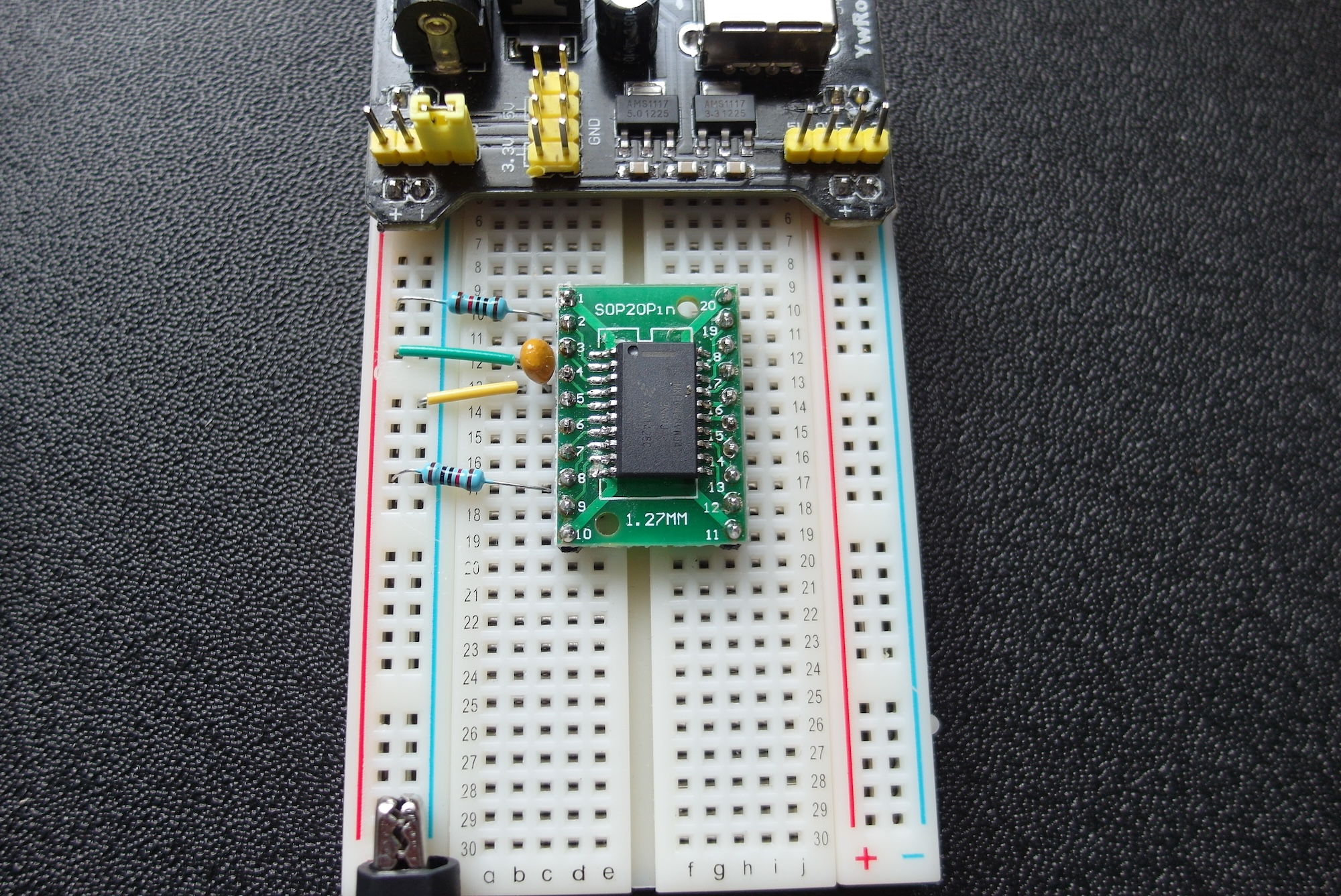
So this time I am attempting to scratch-build a circuit based on a Cortex-M0+ from completely different manufacturer, the Freescale Kinetis KE04. Unlike the NXP parts, this chip has no built-in bootloader, but relies on the “industry-standard” SWD protocol for programming and debugging. Freescale have a huge range of Cortex-M microcontrollers, but the reason I chose this particular one is that it comes in a similar package to the LPC812. I know I can solder this, and I already have a breadboard adapter to fit it.

I am quite familiar with the Kinetis range, having written software to run on their FRDM development boards, but have, so far, never worked with the bare chips. I already have the Freescale FRDM board for this chip, so I reckoned that I might be able to try out some software and the programming connections and protocols on a definitely working board, then try the same approach on my home-built one.

FRDM boards come with a separate MCU on the board just for debugging over USB. As delivered, this emulates a mass storage device. Programming is done by building a binary file, then dragging it onto the device using the host PC’s file management tools. I can see why they do this, as it is pretty much independent of particular development tools. However, I want to build my software in Freescale KDE or Keil uVision and deploy it to the hardware using a generic debug probe.

Testing Kinetis KE04

I started by trying to connect my ULink2 debug probe to the FRDM board, but found a few problems. The first problem was that this device is only really supported by Keil uVision, so I could not easily use any of the software developed using KDE or Freescale CodeWarrior. The second, and more serious problem is that when I opened up my ULink2 to attach the Cortex-M SWD cable, the circuit board did not look much like the pictures on the Keil web site, and there was not even a header to fit the cable. Even though this device has worked well with several STM32 development boards using the 20-pin JTAG connector, I have now come to the tentative conclusion that the one I have my be either a “clone”, or a reduced model which does not support SWD.

SAM_0584

It took me a while to decide that the debug probe might be part of the problem. At the same time I was also poring over datasheets and reference manuals for the KEO4 chip. This was useful, as it suggested that programming would be both easier and more reliable with a 10KOhm pull-up on the RESET and NMI pins and a decoupling capacitor across the power pins. While experimenting, I used an oscilloscope to look at the signals on the pins and saw a strange repeating pattern on the RESET pin, even when pulled up. This puzzled me until I found a page on the Freescale web site and a stack exchange thread which explained that this is very common on new chips, and that any good debug probe should be able to halt the chip and clear the flash memory to stop this behaviour.

Without a working ULink2, one fallback position was to buy a real debug probe. However, a potentially simpler (and cheaper!) alternative would be to update the firmware on the FRDM board to act like the de-facto standard Segger debug probe. Erich Styger at MCU on Eclipse wrote a useful post on how to do this. It seems Segger provides official “OpenSDA” software for this task, and installing it was pretty straightforward. I was soon able to download, run and debug software using both KDE and Keil uVision on the FRDM board. The next step was to connect the re-flashed debug probe to my scratch-built board. To my amazement, it worked, and I was soon running a ‘blink’ program.

SAM_0586

SAM_0588


I was so delighted, that I danced around my workbench a little, then tried again a few times just to make sure things were really working.

There is one fly in the ointment, though, the issue of licence terms and conditions. The licence for the Segger formware for the FRDM boards makes it very clear that it is not to be used with external or custom boards, but only with the chips in situ on the FRDM development boards. So, strictly, by even trying this I was breaking the terms, and this is not an ethical or sustainable way to continue.

Next time I shall look at some other, more legal, ways of using Segger firmware.

ARM Cortex-M board from scratch part 2: LPC810

As I mentioned in my previous post in this series, I have been planning for a long time to make my own ARM Cortex development board from scratch. After a lot of mulling around, and a bit of a false start with the LPC1114 chip, I discovered JeeLabs, a comprehensive web site, blog and upcoming book all about this sort of stuff run by Jean-Claude Wippler. A lot of the older material is based around Atmel AVR chips. Starting in November last year, however, Jean-Claude has been exploring the world of 32-bit ARM, beginning with the cute little LPC810, in a breadboard-friendly eight-pin Dual-in-Line package.

lpc810

This chip is small in both size and features compared to most ARMs, but still packs a surprising amount of punch. It has a Cortex M0+ core running at 25MHz, 4K of flash, 1K of RAM, six GPIO pins, two UARTs, SPI, I2C, several timers and an analogue comparator. All of this is a bit much to squeeze into only eight pins, especially when you consider that two of them are earmarked for power and ground! The way NXP get around this is by providing a built-in switch matrix which can route (almost) any chip feature to any pin. This gives a surprising amount of flexibility for simple applications.

Although the point of this exercise is to build my own development boards, sometimes its comforting to have something to fall back on to test things out. NXP originally produced a nice simple development board for this chip, but sadly it seems that this board is no longer available, so if I am to do anything with this device I will have to make my own.

The first step is to find out a minimum circuit. Luckily, JeeLabs has this covered

NXP LPC810 minimal circuit
Image thanks to jeelabs.org

There are some interesting things about this circuit. The first is the very small number of components There’s the microcontroller itself, a smoothing capacitor for the power pins and an LED. The second interesting thing is the LED. It is mainly used as a rough and ready regulator to drop 5V, provided by a serial adapter board, to 3.3V for the device. For a purely 3.3V circuit, even that would not be necessary! The simplicity of this circuit made me very happy. Surely even I can’t get this wrong! I still have niggling worries about the lack of any pull-up or pull-down resistors on any of the communication pins, but Jean-Claude has obviously made it work. I quickly assembled the specified circuit on a small breadboard, following the JeeLabs instructions.

LPC810 on breadboard

Next came the challenge of programming the LP810. There are so few pins that it does not make sense to permanently dedicate several of them to functions such as RESET and the SWD programming protocol, and not everyone has a SWD debug probe. To help get round this, the LPC810 comes with a built-in bootloader which looks for a particular pattern of highs and lows on some of the pins and switches into a serial programming mode.

If The ISP pin (pin 5) is low when the chip powers up or comes out of reset, it will enter programming mode and expect commands and data over a serial port on pins 2 and 8. While serial port adapters are cheap and plentiful (even though they don’t often have an output which does exactly the right thing for the ISP pin) this approach does mean that some special software is needed which speaks the correct protocol over the serial port. JeeLabs recommends some software called lpc21isp which it recommends installing in a Linux virtual machine. I tried this approach and spent several days messing with software and modified serial adapter boards. All with no success.

In my case it seems that code in a Linux VM was either unable to write to the USB serial port, or suffered timing problems which prevented it form working. Whatever versions I could find for Windows were not quite the same and didn’t work either. Eventually I gave up on the modified serial board approach, and fitted a manual ISP button (initially it was just a jumper cable). This allowed me to, eventually, get some JeeLabs example code onto the chip so I could see it blink an LED. The process still seemed pretty hit or miss, though. A large proportion of the time the software download would fail, with no obvious reason why, and messing with a manual ISP switch became very tedious. I also faced the problem that I was not set up to develop code in the same way as Jean-Claude at JeeLabs, so I was mostly limited to the supplied examples. I even tried connecting my Keil ULink 2 debug proble to the SWD pins, in an attempt to use Keil uVision to write code for this chip. Again without success. Adafruit recommends the LPCXpresso IDE, so I also installed that. Although I could use it to program other NXP chips on pre-made development boards, I still had no real success with programming the LPC810.

LPC812

The LP810 is very sweet, but the small number of available pins does limit its usefulness. After some examples with this little chip, JeeLabs moved on to cover the very similar LPC812, which mainly differs in having a smaller (TSSOP) package with 20 pins. With a bit of care I was able to solder this chip onto a DIP adapter. The extra pins are nice, but I still faced the same issues with programming. I decided that however neat the idea of the ISP pin and serial bootloader seems on the surface, it is just too fiddly for sensible software development.

Next time I’ll step into the confusing world of SWD, but this time I’ll try with a microcontroller where I am already comfortable with the development software.

ARM Cortex-M board from scratch part 1: Too Many Options

As many of my readers will be aware, I have quite an extensive collection of microcontroller development boards with a wide range of controller chips from a variety of architectures and manufacturers. While it’s fair to say that I enjoy programming and creating projects with these boards, there has always been a niggle in the back of my mind that too much of the work has been done for me. Often it’s even worse than that: chip manufacturers delight in cramming boards full of peripherals and options which are great to play with but not much help in learning about the needs of the basic hardware.

SAM_0202

I have come to the conclusion that to really understand things, I need to build my own development board(s) from scratch. A while ago I went down this route with an Atmel AVR microcontroller (as used in the popular Arduino boards) but that is no longer enough. The great majority of my development board collection is based on ARM Cortex-M micro-controllers, so I am determined to get to grips with building and programming my own ARM Cortex-M circuits. Along the way I expect to face the challenges of surface-mount soldering, complex programming protocols, massive documents and differing vendor implementations. If all this works out, I am even dreaming of learning how to design and produce my own printed-circuit boards for whatever I come up with.

Unlike the simpler world of Arduino, there are a multitude of choices when it comes to Cortex-M. ARM itself just sells core designs, it does not make chips – that is left to third parties: anyone who can pay the licence fees to ARM and has the resources to produce and market the silicon. Naturally these manufactures do not all make exactly the same devices. To start with, ARM provides a range of core designs in the Cortex-M series including M0, M0+, M3, M4, M4F and M7. Although broadly compatible, these chips offer different base capabilities. Each manufacturer chooses one or more of these cores and adds their own on-chip circuitry such as UART, SPI and I2C, analogue input and output, timers and so on. Some manufacturers (for example Cypress, in their PSoC range) add all sorts of programmable logic and analogue components, while others stick to simpler, cheaper designs. Each manufacturer also makes choices about power consumption and the ability to “switch off” parts of the chip to consume less.

Freescale_tiny_650_1200

After deciding what micro-controller core to use, choosing extra on-chip circuitry and power controls, there’s still the matter of packaging. ARM Cortex devices are used in a very wide range of situations. Some need to be really tiny, others need lots of pins and power. Unlike more traditional AVR and PIC MCUs, there are hardly any ARMs in “breadboard-friendly” Dual-In-Line (DIP) packages. Luckily, there are a few.

For me, the biggest problem has been finding out what the minimum circuit for a given chip might be. I view this as the electronics equivalent of ‘Hello World’ or ‘blink’ in the software world. When starting out there are far too may choices to make. As well as which controller chip, there’s how to wire it up to power and stuff, pull ups and pull-down resistors, capacitors and crystals, how to connect it to some sort of programmer, which programmer to use, which development software to use, and what to write to exercise the system. I always prefer to learn by starting with a bare minimum working design and making and testing small changes until I get to where I want. In the embedded design world this does not seem a very common approach. Instead, we are presented with huge technical references and datasheets, with no worked examples, which just reveal even more options to get wrong.

What I really want is a guaranteed minimal circuit to start with, so that if the device won’t start or won’t program, I know the problem is elsewhere. My naive assumption was that each manufacturer would obviously produce an ‘application note’ with such a minimal circuit, but no. I may be looking in the wrong place, but so far I have not found such a document from any manufacturer. I even bought some ’embedded system design’ books in the hope that they might help, but they all start with software, and just assume that all the electronics is already in place.

With no apparent support from the manufacturers, I am left looking to the web for help. To try and eliminate PCB design from the problem, I plan to start with one of the few DIP ARM chips, and see how far that will get me.

NXP LPC1114 Dual in Line ARM chip

The first obvious choice is the NXP LPC1114. The micro-controller community got quite excited whe NXP released this part, and on the surface it looks like a good choice. Plenty of people have had a go at it and there seem to be quite a lot of web resources. There’s one big problem, though. The chip itself is very hard to come by. None of the usual suppliers seem to stock it, leaving only a small collection of ebay vendors. I eventually managed to get hold of one for a mostly reasonable price, but so far I have not yet dared to try and program it in case I kill it!

It took me several months of indecision before I finally discovered some very helpful resources about another NXP chip, the LPC810. This is a much smaller DIP package with only 8 pins, not enough for even a basic JTAG connector, so it uses its own bootloader firmware. Next time, I’ll cover my adventures with LPC810, and its close cousin LPC812.

A handy (and cheap) gadget for holding small PCBs

For the hundredth time I found myself trying to solder some small circuit board and annoyed by the way it skittered across my desk. I had tried ‘helping hands‘ but these are fiddly and annoying to set up, the screws keep coming loose, and they hold the boards at wonky angles. I had just about given up, so I looked on the web for some sort of PCB clamp or vice.

Circuit Board Holder

Web sites typically seem to recommend ‘panavise‘ brand but these seem pretty expensive and hard to get outside the USA. In a previous job we used a very clever system which clamped the PCB for component placement and also allowed it to be flipped over for through hole soldering, but this sort of thing is even more expensive. However, I looked a bit further and found an interesting little gadget for under £3 including delivery on ebay. I ordered one from a printed circuit board shipping company and it arrived the next day.

Circuit Board Holder with FRDM KE04Z board

The device is all metal, and reassuringly heavy with rubber feet and even screw holes to fix it. There’s no way it will move, even under the most forceful electronics work. placing and removing boards for work is simple, just pull back the spring-loaded clip. It seems fairly adjustable for a variety of board shapes, but is obviously limited to boards small enough to fit. I have tried it with a selection of Freescale FRDM boards, Arduinos of various sizes as well as Raspberry Pi main boards, expansions and HATs and it comfortably held all of them. Something like a Gertboard would be too big, though. The device is designed for phone repair where everything is low-profile, so there’s also a chance that some boards with lots of tall components might not fit properly because they bump into the central metal support bar.

I’m hoping that the metal bottom plate will also help spread waste heat from hot-air reflow soldering and unsoldering of surface-mount parts, but I haven’t tried that yet.

Arduino development in a web browser

Over the last few years I have written and edited many Arduino sketches. Aside from a brief dalliance with Sublime Text I have exclusively used the dull but ubiquitous Arduino IDE.

At the time I started each project this seemed completely natural, but over time I seem to somehow lose track of where I put the code. I use a variety of different computers, including virtual ones, several file sharing and backup systems (Dropbox, Google Drive and Bittorrent Sync, for example) and a heap of removable media. Many of my ‘important’ sketches are version controlled and stored in GitHub or BitBucket. Somewhere in that lot is probably something useful for my next project, but it’s getting tougher and tougher to find it.

With all this in mind I am excited to have found Codebender – a browser-based Arduino IDE which backs up all your sketches to ‘the cloud’ and is available from any computer with an internet connection. Strictly it also needs, for the moment at least, a Chrome browser if you want to run the plugin which recognizes, controls and communicates with your Arduino hardware. I use Chrome most of the time anyway, so that’s not really a problem for me.

Codebender

I have now uses Codebender heavily for a couple of projects, and found it smooth to use and somewhat easier to get to grips with than the original Arduino IDE. It recognizes and works with a large and growing collection of Arduino boards and compatibles, but it does not currently support non-AVR systems (Arduino Due and other ARM boards, Iteaduino Lite and boards with AVR-clone controllers, for example). It also has access to a large collection of libraries.

Interaction between the web interface and the Arduino is generally seamless, provided you have a reliable internet connection. I did find that I had sometimes to re-try programming the hardware when I was in an area with intermittent wi-fi, but none of my source code was lost and the second download attempt usually worked.

If you are like me, and hop from one machine to another, or even if you are just a bit tired of the quirks of the Arduino IDE, I recommend that you sign up for Codebender. It’s free, and it might be useful.

For full disclosure, if you sign up using the links I give above, I get some points. If I get enough points, I might get a free T-shirt. Despite that, I still think this is a worthwhile service to try.